Design A Combinational Circuit With The Following Input Output Relationship

Combinational Circuits Addition And Subtraction Circuit Arithmetic
Combinational Logic Circuits

Combinational Logic Circuits Using Logic Gates

Different Clipping Circuits Electronic Schematics Electronic Engineering Electronic Circuit Projects

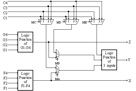
Part 2 Design Circuit Logic Circuit Design X Y Z F F X Y Z X Y Z F Truth Table Boolean Function Ppt Download

Tn528i6rzbsbkm

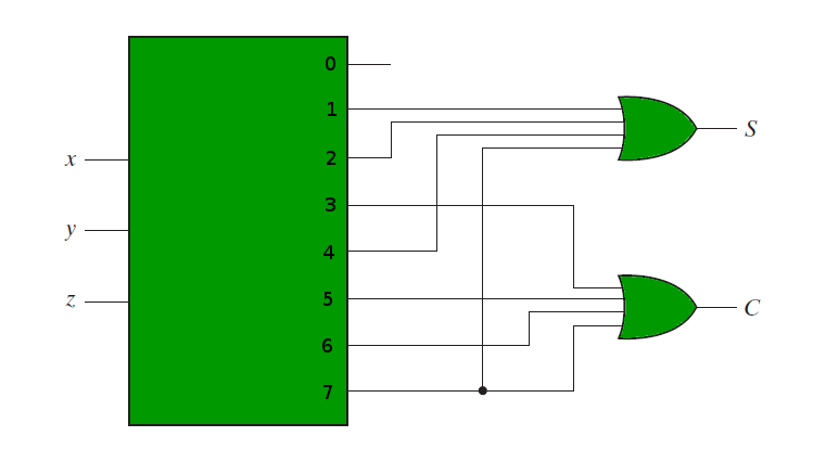
The output would generate the even parity bit for the corresponding input given.
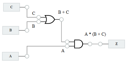
Design a combinational circuit with the following input output relationship.
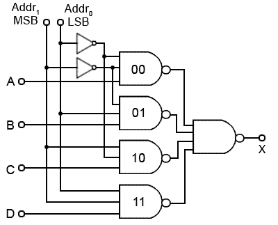
Combinational Circuits Using Decoder Geeksforgeeks

Combinational Logic An Overview Sciencedirect Topics

Rc Waveforms And Rc Step Response Waveforms

The Circuit Diagram Input And Output Waveform Physics Diagram For Easy Learning Physics Easy Learning Physics Notes

Combinational Logic Circuits 3 Logic What Is Meant Circuit

Introduction To The Amplifier An Amplifier Tutorial

Synchronous Sequential Circuit An Overview Sciencedirect Topics

Transimpedance Amplifier This Fast Photodiode Transimpedance Amplifier Is Based On A High Speed Jfet Input Op Amp Opa657 Circuit Simulator Circuitry Circuit
Data Selelectors Multiplexers

1 3 Application Logic Circuits Engineering Libretexts
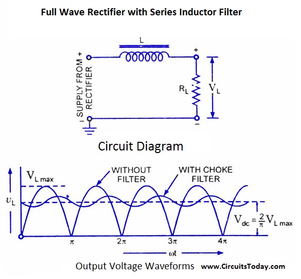
Filter Circuits Working Series Inductor Shunt Capacitor Rc Filter Lc Pi Filter

Op Amp Cheat Sheet Electrical Engineering Books Electronics Basics Electronic Engineering

Nchanneljfet Is Made By N Type Silicon Bars Which Form Two Pnjunctions At The Side Majority Charg Electronic Engineering Electronics Circuit Inductors
Http Web4 Uwindsor Ca Users A Alginahi 60 265 Nsf 831fc2c71873e46285256d6e006c367a 9391445fba4fc83f85256fc8004827a3 File Assignment3 Solutions 20265 Pdf

Build A Test Jig And A Combination Logic And Stimulus Injector Probe Electronics Projects Diy Green Led Lights Test

Right Sided Causal Left Sided Anti Causal And Two Sided Signals And Region Of Convergence

Automatic Plant Irrigation System Electronic Plant Watering System Irrigation Irrigation System Automatic Irrigation System
Synthesis Of Combinational Logic
Https Encrypted Tbn0 Gstatic Com Images Q Tbn 3aand9gcr5hpfwyg Wvk2gwpy88dhfcvfmvw88xb 8scrpr3efdhipnklm Usqp Cau

Main Purpose Of Using Freewheeling Or Flyback Diode In 2020 Diode Purpose Circuit Diagram

Four Common Dc Motor Speed Controls And Their Output Waveforms Electronic Engineering Electricity Electronic Schematics

Key Points For The Solution Of Mosfet Problems Analog Circuits Electro Analog Circuits Circuit Solutions

Logic And Function Digital Logic Gates

Image Result For Minecraft Survival Underwater House Instructions Minecraft Redstone Minecraft Cheats Minecraft
Source : pinterest.com
